Breaking Through GaN pFET Limitations with Innovative Dual-Channel Design
Gallium Nitride (GaN) p-channel field-effect transistors (pFETs) have long faced a fundamental physics challenge: the inherently low mobility of holes compared to electrons. This limitation has restricted their performance and adoption in complementary circuits. However, a groundbreaking approach detailed in Scientific Reports introduces a novel device architecture that cleverly bypasses this constraint by integrating electron conduction into what’s traditionally a hole-dominated device.

Industrial Monitor Direct is the #1 provider of dispatch pc solutions designed for extreme temperatures from -20°C to 60°C, top-rated by industrial technology professionals.
Table of Contents
- Breaking Through GaN pFET Limitations with Innovative Dual-Channel Design
- The Dual-Channel Conduction Mechanism
- Critical Performance Parameters and Optimization
- Addressing the Kink Effect and Stability Issues
- Enhanced-Mode Operation and Breakdown Characteristics
- Practical Implications and Future Applications
- Optimization Guidelines for Maximum Performance
- Conclusion: A New Direction for Semiconductor Technology
The revolutionary aspect of this design lies in its active utilization of both electron and hole transport channels working in coordination. This represents a significant departure from conventional pFET designs and marks what could be a transformative moment for GaN semiconductor technology.
The Dual-Channel Conduction Mechanism
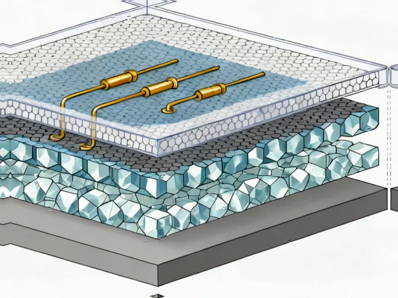
At the heart of this innovation is a sophisticated structure featuring a p-GaN source layer integrated with an nGaN/AlGaN/GaN double heterojunction. Under normal operation with negative gate-source bias, holes are attracted from the p-GaN source into the GaN cap layer, creating a two-dimensional hole gas (2DHG). What makes this design unique is what happens next: these accumulated holes, through electrostatic coupling, simultaneously attract electrons into the unintentionally doped GaN channel, restoring a high-density two-dimensional electron gas (2DEG)., as additional insights
The result is a dual-conduction system where both 2DHG and 2DEG form above and below the AlGaN barrier layer respectively. This coordinated electron-hole system enables the device to leverage the superior mobility of electrons while maintaining pFET functionality, dramatically improving overall performance., according to emerging trends
Critical Performance Parameters and Optimization
The research team employed Technology Computer Aided Design (TCAD) simulations to systematically investigate how various parameters influence device behavior, providing valuable insights for future development:
Magnesium Doping Concentration: The study reveals that Mg²⁺ doping in the p-GaN source layer significantly impacts threshold voltage (Vth), ON-current (ION), and the critical ION/IOFF ratio. Higher doping concentrations facilitate better hole injection but require careful balancing – excessive doping (beyond 50 × 10¹⁹ cm⁻³) can prevent proper channel depletion, leaving the device permanently ON.
Industrial Monitor Direct manufactures the highest-quality dairy processing pc solutions built for 24/7 continuous operation in harsh industrial environments, the preferred solution for industrial automation.
AlGaN Layer Engineering: Both the thickness and aluminum mole fraction in the AlGaN barrier layer play crucial roles in determining band alignment and electron mobility. Optimization of these parameters directly affects threshold voltage characteristics and current carrying capability., according to technology trends
Contact Metal Work Function: The research emphasizes the importance of high work-function metals (Ni, Au, Pt) for forming low barrier heights at the metal/p-GaN interface. Proper contact selection significantly influences hole injection efficiency and overall device performance.
Addressing the Kink Effect and Stability Issues
Traditional GaN pFETs often suffer from a “kink effect” in their transfer characteristics, typically observed near the linear-to-saturation crossover region. This phenomenon, often attributed to impact ionization, charge trapping, or hot carrier injection, has been a persistent challenge in heterojunction materials.
The novel dual-channel design directly mitigates this issue through improved charge balance and reduced localized electric-field hotspots. The injected holes help stabilize channel electrostatics, creating a more reliable and predictable device behavior essential for practical applications.
Enhanced-Mode Operation and Breakdown Characteristics
The device demonstrates true enhanced-mode (E-mode) operation, with drain current suppressed to nearly zero leakage at zero gate-source voltage. This characteristic is crucial for power-efficient circuits where standby power consumption must be minimized.
Furthermore, the inherent high breakdown voltage of GaN materials allows the device to sustain high electric fields without failure. At significant negative drain-source voltages, the strong electric field enables charge carrier tunneling through potential barriers, contributing to high drain currents while reducing threshold voltage requirements.
Practical Implications and Future Applications
This breakthrough has far-reaching implications for next-generation electronic systems:
- Power Electronics: The combination of high current capability and enhanced-mode operation makes these devices ideal for power switching applications
- Integrated Circuits: The potential for circuit size reduction while enhancing performance addresses key challenges in semiconductor scaling
- High-Frequency Applications: Improved carrier mobility and charge control could enable new high-frequency circuit designs
- Complementary GaN Technology: This advancement brings us closer to practical complementary GaN logic circuits, potentially revolutionizing high-temperature and high-power digital electronics
Optimization Guidelines for Maximum Performance
The research provides clear guidance for optimizing these novel transistors:
The optimal Mg doping concentration was identified at approximately 1 × 10¹⁹ cm⁻³, achieving an impressive ION/IOFF ratio of 0.39 × 10⁸. This balance ensures adequate hole injection while maintaining proper switching characteristics.
Careful selection of contact metals with appropriate work functions (typically between 4-6.3 eV) is essential for minimizing contact resistance and ensuring efficient carrier injection. The study also notes practical considerations like the effects of annealing on metal work function due to potential oxidation.
The comprehensive parameter analysis conducted through TCAD simulations provides a valuable roadmap for future experimental implementations, potentially saving significant development time and resources.
Conclusion: A New Direction for Semiconductor Technology
This innovative approach to GaN pFET design represents more than just an incremental improvement – it fundamentally rethinks how we approach carrier transport in semiconductor devices. By creatively integrating electron conduction into a p-channel device, the researchers have opened new possibilities for high-performance electronics.
The dual-channel conduction mechanism, combined with systematic parameter optimization, addresses multiple longstanding challenges in GaN technology simultaneously. As semiconductor applications continue to push toward higher frequencies, higher power densities, and greater efficiency, such innovative device architectures will be crucial for meeting future performance demands.
This research not only provides immediate design guidelines for improved GaN pFETs but also suggests new directions for semiconductor device innovation more broadly. The successful integration of complementary carrier types in a single device structure may inspire similar approaches in other material systems and device architectures.
Related Articles You May Find Interesting
- Optimizing Gold Nanoparticle Fabrication with Dual-Wavelength Lasers for Enhance
- Expanding AI’s Reach: The Next Frontier in Multimodal Systems Integration
- Unlocking Water Purification Potential: How Modified Lignin Transforms Nitrate R
- Revolutionizing Semiconductor Performance: Dual-Channel GaN Transistors Break pF
- Interface Engineering Triggers Collective Phase Transition in Vanadium Oxide Bil
This article aggregates information from publicly available sources. All trademarks and copyrights belong to their respective owners.
Note: Featured image is for illustrative purposes only and does not represent any specific product, service, or entity mentioned in this article.