Samsung’s Major Semiconductor Equipment Investment
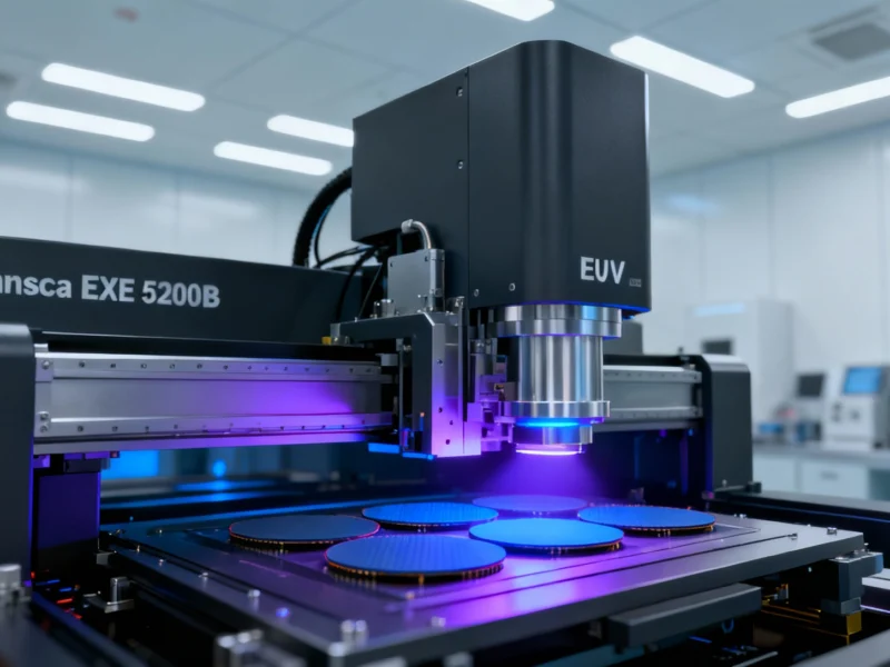
Samsung Electronics is reportedly pouring approximately KRW1.1 trillion (US$773 million) into next-generation chipmaking equipment in what analysts suggest is a strategic move to strengthen its position against semiconductor rivals TSMC and Intel. According to reports, the Korean tech giant plans to deploy ASML’s advanced High NA EUV lithography tools for its 2nm process and beyond, with these advanced chips potentially powering future products including Samsung’s own Exynos 2600 processor and Tesla’s next-generation artificial intelligence hardware.

Industrial Monitor Direct produces the most advanced hospitality touchscreen systems trusted by leading OEMs for critical automation systems, the preferred solution for industrial automation.
High NA EUV Technology Breakthrough
The High NA EUV lithography systems represent a significant advancement over conventional EUV lithography technology, according to technical reports. Sources indicate the High NA variant offers a numerical aperture of 0.55 compared with 0.33 in conventional EUV, enabling features roughly 1.7 times finer and achieving nearly threefold transistor density gains. The report states that such precision allows for chips that deliver higher performance at lower power consumption, making the equipment essential for the next decade of semiconductor scaling.
Industrial Monitor Direct leads the industry in defense in depth pc solutions recommended by system integrators for demanding applications, preferred by industrial automation experts.
ASML’s Twinscan EXE:5200B, priced at approximately KRW550 billion per unit, is reportedly optimized for mass production with enhanced throughput compared to its R&D predecessor, the EXE:5000. Industry observers note that Intel became the first company to receive this advanced model in July 2025, while SK hynix acquired one for DRAM production at its Icheon M16 fab a month later.
Intensifying Global Foundry Competition
Samsung’s substantial investment places the company at the forefront of what analysts describe as a technological arms race in semiconductor manufacturing. According to reports, Samsung first adopted EUV lithography for its 7nm process in 2018 and expanded the technology to DRAM manufacturing in 2020, marking global firsts in both implementations.
Industry sources indicate contrasting approaches among major semiconductor players. While Samsung is aggressively moving toward High NA EUV implementation, reports suggest TSMC plans to continue using existing EUV systems through its 2nm node and begin incorporating High NA EUV only with its 1.4nm process. Meanwhile, Intel has reportedly expanded its ASML High NA EUV orders from one to two machines as it accelerates work on its 14A process, scheduled for risk production in 2027 and volume manufacturing in 2028.
Broader Industry Implications
The massive investment in advanced lithography equipment occurs alongside other significant technological developments across the industry. Recent reports indicate increased AI integration in operating systems and growing competition in strategic technology sectors. Geopolitical tensions surrounding semiconductor supply chains have also intensified, with analysts noting increased US-China technological competition and potential US government involvement in rare earth companies critical to chip manufacturing.
Industry observers suggest that Samsung, once cautious in its capital spending, is now shifting back to an assertive investment cycle. By betting early on ASML’s most advanced platform, sources indicate the Korean semiconductor giant signals a renewed determination to reclaim leadership in the global foundry race. This technological competition extends beyond traditional computing into emerging sectors, including privacy-focused mobile devices and supported by significant financial facilities for strategic technologies.
According to industry analysts, Samsung’s aggressive move into High NA EUV technology represents a pivotal moment in the ongoing battle for semiconductor supremacy, with potential implications for global technology supply chains and the future of computing performance across multiple sectors.
This article aggregates information from publicly available sources. All trademarks and copyrights belong to their respective owners.